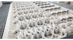
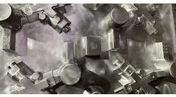
A series of ceramic molds formed by LAMP directly from CAD data.
Investment casting remains the foundry industry’s cutting edge, but it may yet get better — faster, and less cost-intensive. Researchers at the Georgia Institute of Technology have developed a technology that could change how complex parts are designed, speed up prototype development, and accelerate production planning. Prof. Suman Das has developed an all-digital approach that allows a part to be made directly from its CAD model. The project has received $4.65 million in U.S. Dept. of Defense funding from the Defense Advanced Research Projects Agency (DARPA.)
“We have developed a proof-of-concept system which is already turning out complex metal parts, and which fundamentally transforms the way that very high-value castings are made,” according to Das, who directs the Direct Digital Manufacturing Laboratory at Georgia Tech’s Manufacturing Research Center (MaRC). “We’re confident that our approach can lower costs by at least 25% and reduce the number of unusable waste parts by more than 90%, while eliminating 100% of the tooling.”
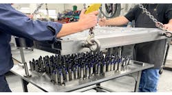
The researchers are studying the way that investment-casting molds are made — the ceramic investment process that converts a wax shape into a ceramic mold. The Georgia Tech researchers are particularly focused on investment cast parts for turbine engine airfoils, working in collaboration with the University of Michigan and PCC Airfoils, an Ohio investment caster. Das pointed out that once a CAD model is finished there are still several important steps to complete before a finished part is ready, involving precision machining of dies and many dozens of tooling parts. “The result is a costly process that typically produces many defective molds and wasted parts before a useable prototype is achieved,” Das said. “This trial-and-error development phase often requires many months to cast a part that is accurate enough to enter the next stage, which involves testing and evaluation.”
The new approach, called “large area maskless photopolymerization” (LAMP), builds a ceramic mold directly from a CAD record, completing the procedure faster and producing fewer wasted parts. It’s a high-resolution, digital process that projects bitmaps of ultraviolet light onto a mixture of photosensitive resin and ceramic particles, and then selectively cures the mixture to a solid so that the mold structure is built accretively, layer by layer.
The LAMP technique layers 100-micron sheets of the material on top of each other until the mold structure is formed. Then, the cured resin is removed by binder burnout and the ceramic that remains is sintered in a furnace. The result is a fully ceramic mold that can receive molten metal to form an accurate casting, even in difficult materials like nickel-based superalloys or titanium-based alloys.
“The LAMP process lowers the time required to turn a CAD design into a test-worthy part from a year to about a week,” Das claimed. “We eliminate the scrap and the tooling, and each digitally manufactured mold is identical to the others.”
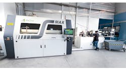
Currently, a prototype LAMP alpha machine is building six, typical turbine-engine airfoil molds in six hours. Das predicted that a larger beta machine, built at Georgia Tech and set for installation at a PCC Airfoils, would produce 100 molds at a time in about 24 hours. Although the focus now is on high-value aerospace parts, the potential for high-volume production suggests applications for many other types of precision metal parts. And, such an impact on production would influence both the design of metal parts, with industrial and commercial implications too, Das observed.
“This process can produce parts of a complexity that designers could only dream of before,” he said. “The digital technique takes advantage of high-resolution optics and precision motion systems to achieve extremely sharp, small features — on the order of 100 microns.”
Das also noted that the new process not only creates testable prototypes but also could be used in manufacturing, as a new entry to the field of rapid manufacturing.

